
So today we will discuss about the pins of 8085 microprocessor. It is an 8 bit microprocessor make by N-MOS technology, It has 40 pins and 256 number of opcodes. So let’s see 8085 pin diagram.
The picture shows a schematic diagram of intel 8085.The details of various pins are given below.
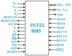 So in this pin configuration, AD0 — AD7 = 8 pins and A8 — A15 = 8 pins total is 16 pins. leaving AD0 — AD7 and A8 — A15 there are 24 pins in total so now there are 16 + 24 = 40 pins.
So In the above pin configuration input pin is 22 and the output pin is 18 total 40 pins.
Address bus and data bus – 8085
Since the microprocessor is a 8 bit, The data bus is of 8 bit size and the address bus is of 16 bit size.
A8 — A15 ( Output ) : The 8 most significant bits ( MSB ) of the address are transmitted by the address bus pins A8 — A15 .
AD0—AD7 ( Input / Output ) : The 8 least significant bits ( LSB ) of the address are transmitted by address or data bus address bus pins AD0 — AD7 .
ALE ( Address latch enable )
It is an address latch enable signal it goes high during the 1st clock cycle of a machine cycle. And enables the lower 8 bits of address to be latch either into the memory or external latch.
IO / M
It is a status signal indicating whether the address is for memory or for input output. When it goes high the address of the address bus is for the input device. When it goes low it is for the address memory location on the address bus.
S0 , S1
So these are status signal sent by the microprocessor to differentiate different types of operation. Given in the table below.
| S1 | S0 | Status |
| 0 | 0 | HALT |
| 0 | 1 | READ |
| 1 | 0 | WRITE |
| 1 | 1 | FETCH |
READY
It is use by the microprocessor to know whether a peripheral/external device is ready to transfer data or not. A slow external device can be connected to the microprocessor through ready line.
If READY is high then the external device is ready and if it is slow then the microprocessor waits until it becomes high.
RD (Read)
So this is a signal to control the READ operation. When it goes low the selected memory or input output device is read.
WR (Write)
So this is a signal to control the WRITE operation. When it goes low the data on the data bus is written on the selected memory or input output device.
HOLD
This indicates that another device is requesting the use of the address and data bus. When the hold signal is sense by the microprocessor, the address bus, data bus, RD, WR and IO/M are tristate.
When the microprocessor receives the hold signal, it stops using the buses as soon as the current machine cycle is completed.

HLDA
So this is a signal for HOLD acknowledgement. It indicates that the HOLD request has been received.
So the HLDA is reduce after removing the hold request. After the HLDA is low, the CPU takes the buses in a half clock cycle.
Interrupt Signal – 8085
The interrupts are mainly interrupt the processing of a microprocessor from a fixed location in the memory. So there are mainly 5 types of interrupts TRAP, RST 7.5, RST 6.5, RST 5.5 and INTR.
The TRAP has the highest priority and it is a non maskable interrupt but The INTR has the lowest priority and it is a vectored interrupt.
TRAP, RST 7.5, RST 6.5, RST 5.5 are all called vector interrupt. And RST 7.5, RST 6.5, RST 5.5 all these are maskable interrupt.
| Interrupt | Corresponding memory location from which operation status |
| TRAP | 0024 H |
| RST 7.5 | 002C H |
| RST 6.5 | 0034 H |
| RST 5.5 | 003C H |
INTR
So this is an interrupt request signal. When it goes high it has the lowest priority among interrupts. So the microprocessor suspends its normal sequence of instructions. And so after completing the instruction it goes to the interrupting device.
INTR’
So it is the interrupts signal send by a microprocessor after INTR is receive.
RESET IN
So this program resets the counter to zero. As long as RESET is applied, the CPU is kept in the reset state. And so it never affects any flags.
RESET OUT
So this indicates that the CPU is being reset.
X1 & X2
So these are the terminals to be connected to the external crystal oscillator which drives the internal circuit of the microprocessor to produce a suitable clock.
CLK ( Clock output )
This is a clock output for the user that can be use for other digital IC acknowledgement. So its frequency is similar to that of a microprocessor.
SID ( Serial input data )
The data on this line is loaded into the 7th bit of the accumulator, when RIM instruction is executed.
SOD (Serial output data )
The 7th bit of the accumulator is output on SOD line when SIM instruction is executed.
VCC + 5 volt supply
VSS ground reference.
| RIM – Read interrupt mask SIM – Set interrupt mask |
Multiplexing – ( Address bus / Data bus )
The address or data bus transmits data and address at different movement at a particular movement it transmit either data or address, So the address bus operates in time share mode this technic is know as multiplexing.
If you want more information, then click on the article given below
So in the above article we read about pin configuration of intel 8085. And also read its status signal, reset signal, serial I/O signal and function of ALE. I hope that you will get a lot of information from this topic, So this is all about of 8085 pin configuration, Thank you.