
Here we are going to talk about Intel 8255 programmable peripheral interface (PPI). It is a multiport peripheral device, Its main function is to interfacing external microcomputer. And it has three 8-bit ports and that is (i) Port A (ii) Port B (iii) Port C. The port ‘C’ has been further divide into 2 parts, one is port Cupper ( 4-bit ) and the other is port Clower ( 4-bit ) overall 8-bit. Hence the port ‘C’ is 8-bit. So it can be use input port either output port.
Architecture of Intel 8255 microprocessor
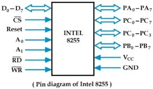
It is a 40 pin I. C. package. It operates on in single +5 volt DC supply.
The pins for various ports are
- PA0 − PA7 ( 8 pins of port A )
- PB0 − PB7 ( 8 pins of port B )
- PC0 − PC3 ( 4 pins of port Clower )
- PC4 − PC7 ( 4 pins of port Cupper )
Click for Flags in 8085 microprocessor.
Block diagram of Intel 8255

So the important control signals are CS (Chip select), RD (Read), WR (Write), A0 and A1.
CS ( Chip select ) :
The low status of the signal enables communication between CPU and 8255.
RD ( Read ) :
When read bar goes low the 8255 sends out data or status information to the CPU on the data bus. It allows the CPU to read data from the input port of 8255.
WR ( Write ) :
When write bar goes low the CPU writes data into 8255. The CPU writes data into the output port of 8255.
A0 and A1 :
The selection of input port and control word register (CWR) is done using A0 and A1 pin in conjunction with read bar and write bar. So A0 and A1 are normally connect to the least significant beat (LSB) of the address bus.

If we write the instruction IN00 it means that it is for port ‘A’ of 8255. When this instruction is executed data are transfer from port ‘A’ to the accumulator.
Similarly OUT 03 it will transfer the content of the accumulator to the control word register of 8255. The IN instruction is use for the port which has been defined as IN port.
After the IN the address of the port is specified. Similarly OUT instruction is use for the ports which have been define as OUT port. For control word register only OUT instruction is use.
Click for 8085 pin diagram.
Intel 8255 operating modes
The Intel 8255 has the following three modes (1) Mode 0 — (Simple input or output) (2) Mode 1 — (Strobed input or output) and (3) Mode 2 — ( Bidirectional port / Strobed bidirectional mode ).
Mode 0 — Simple input or output
In mode – 0 operation a port can be operate as simple input or output port. Each of the 4 ports of 8255 can be program to be either an input or output port.
Mode 1 — Strobed input or output
Port A and B both are design to operate in this mode. When port A and port B are program in mode – 1, 6 pins of port C are use for their control.
PC0 , PC1 and PC2 are use for the control of port B which can be use either as input or output port. If port A is operate as an input port PC3 , PC4 and PC5 are use for its control.
The remaining pins of port ‘C’ that is PC6 and PC7 can be use as either input or output. When port A is operate as in output port pins PC3 , PC6 , and PC7 are use for its control.
And the pins PC4 and PC5 can be use either as an input or output. The combination of mode – 1 and mode – 0 operation is also possible. For example when port A is programmed to operate in mode – 1 the port B can be operate in mode – 0.
Mode 2 — Strobed bidirectional mode
This mode – 2 operation is only for a port A. So here the port A can be program to operate as a bidirectional port.
When port A program in mode – 2 the port B can be use in either mode – 1 or mode – 0. For mode – 2 operation PC3 to PC7 are use for the control of port A.
What is control word in microprocessor ?

Bit number 0 :
It is for port Clower . To make port Clower an input port the port set to 0. To make port Clower an output port the bit set to 0.
Bit number 1 :
It is for port B. To make port B and input port is set to 1. To make port B and output port the bit set to 0.
Bit number 2 :
It is for the selection of the mode for port B. If the port B has to operate in mode – 0 the bit is set to 0. For mode – 1 operation of mode B it is set to 1.
Bit number 3 :
It is for port Cupper . For input set to 1. For output set to 0.
Bit number 4 :
It is for port A. similarly, for input it is 1 and for output it is 0.
Bit number 5 & 6 :
So these bits are to define the operating modes of port A.

Bit number 7 :
If port A ,B and C are define as input or output port. So It set to 0 If the individual pins of the port C are to be set or reset. So It is set to 0.
Example 1 : Make control word when the ports of 8255 are define as follows.
- Port A as an input port.
- Mode of the port A , mode 0.
- Port B as an output port .
- Mode of port B, mode 0.
- Port Cupper as an input port.
- Port Clower as an output port.

Example 2 : From control word of the following configuration of the codes 8255 for mode 0 operation.
(i) Port A output (ii) Port B output (iii) Port Clower output (iv) Port Cupper input

So in the above post got to know about Intel 8255 PPI. And we also got to learn each function of its block diagram and its pins, 3 operating modes, control word work, architecture of 8255. So this is all about Programmable Peripheral Interface 8255. I hope that i have given good information to you guys.