
Most semiconductor devices have one or more PN junction. PN junction are of great importance because they are actually the control elements for semiconductor devices. In – depth knowledge of the formation and properties of PN junction enables the reader to understand the operation of semiconductor devices.
So let’s know a little more about PN junction. First of all we see what is the definition of PN junction.
Definition of PN Junction :
When a P – type semiconductor suitably connected to an N – type semiconductor the contact surface is known as PN junction.
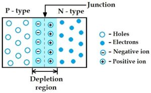
In the p-type semiconductor the majority charge carries are represent by holes. Holes are the vacant place created by the loss of electron.
N – type semiconductor has majority charge carries has electrons which are negative charge particle. When P – type semiconductor is made to join with N – type.
The free electrons from N – type diffuse towards P – type semiconductor. This diffusion of electrons make the recombination of electrons and holes.
Due to this the positive ion of N – type semiconductor are create near the junction. This ion are immobile and offer a barrier (oppose) to the diffusion of further electrons.
This barrier is know as potential barrier of the P – N junction. And this region is also know as depletion region.
Because the region contain only immobile ion. And this region free mobile charge carriers like electrons and holes.
Click For what are the classification of electronic materials
Biasing in PN junction
Definition of Biasing : The process of applying external DC voltage to an electronic device is know as biasing.
Biasing are of two types that is
- Forward biasing
- Revers biasing
Forward biasing of p-n junction

When the positive terminal of the battery connect to the P – type. And negative terminal of the battery is connect to the N – type of the PN junction then it is know as forward biasing.
The width of the depletion layer decrease and so the current flow through the junction. As potential barrier voltage is very small therefore a small forward voltage is sufficient to completely eliminated the barrier.
Once the potential barrier is eliminate by the forward voltage junction resistance becomes almost zero, therefore current flow in the circuit.
In N – type region current is carries by free electrons where as an P – type region it is carries by holes. The current which flow in forward biasing is know as forward current ( If ).
Reverse biasing of PN junction

When negative terminal of the battery is connect to the P – type. And positive terminal of the battery is connect N – type of the P – N junction then it is know as reverse biasing.
In case if reverse biasing the width of the depletion layer increase. Hence the current through the junction is almost zero (0) or negligible.
This negligible current is know as leakage current (Ir ) the apply reverse voltage establishes and electric field which act at in the same direction as the potential barrier therefore barrier is increase.
The increase potential barrier remains the flow of charge carriers across the junction, hence no current will flow.
Explain the formation of p-n junction
The common method of making P-N junction is know as alloying. In this method a small block of indium is place on an N-type germanium slab.
The system is being heated the temperature about 500° c. The indium and sum of the germanium melt to form a small puddle of molten germanium indium mixture.

The temperature is name lower and puddle beings to solidified, under proper condition. The atoms of indium impurity will be suitable adjust in the germanium slab to form a single crystal.
The addition of indium overcome the excess of electrons in the N-type germanium. So to such an extern their re-creates a P-type region.
The remaining molten mixture appears as indium button. And this button serves as a suitable base cause soldering leads.
Properties of PN junction
At the instant of PN junction formation the free electrons near the junction in the N-region being the diffuse across. The junction in to the P-region, where the combine the hole near junction.
The result is that an region losses free electrons as they diffuse in to the junction. This creates a layer of positive charges near the junction at the same time.
The P-region loss holes as the electron and holes combine and this creates the layer of negative charges near the junction. The two layers of positive and negative charges form the depletion region or layer.
Once P-N junction is form and depletion layer crated the diffusion or free electrons stop. Their exist a potential difference across the depletion layer is know as depletion potential or barrier potential.

Explain the VI characteristics of PN junction diode
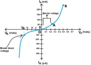
V – I characteristics of a semiconductor diode is the graph between voltage applied and current through the diode. Voltage is always taken in horizontal ( X – axis ) and current is represent in vertical ( Y – axis ).
We have to draw the graph by making the diode forward bias for positive voltage. And for the negative voltage the diode make by reverse bias.

V-I characteristics of forward bias
Under forward bias condition the depletion layer width is small. So less voltage is require to overcome the potential barrier or surface barrier.
A some forward voltage ( 0.7 volt for silicon and 0.3 for germanium ) The potential barrier is all together eliminate and current starts flowing in the circuit.
The current increases with the increasing in the forward voltage. Thus a raising curved is obtain with forward bias. It is seeing that at first region ( OA ).
The current increases very slowly and the curve is non – linear. Once the external applied voltage axis the potential barrier voltage
And the PN junction behaves like an ordinary conductor. Therefore the current raises very sharply with increase external voltage.
V-I characteristics of reverse bias
When negative voltage is apply to the PN Junction diode, The depletion layer width is increased. Hence no current flow through it. But in particles a very small current ( micro ampere ) flow in the circuit.
This current know as reverse saturation current and due to minority carriers. If reverse voltage is increase continuously then the kinetic energy of electrons may be come very high.
To not out electrons from semiconductor atoms. At this place breakdown of the junction occurs. Due to sudden rise of reverse current and this may destroyed the junction permanently.
Under zero ‘0’ external voltage
When the external voltage is zero (0) that is the circuit is open ‘K’. The potential barrier at the junction does not permit current flow therefore the circuit current is zero.
Click for types of electron emission.
Some important notes : –
Breakdown voltage in PN junction
It is the minimum reverse voltage at which PN junction breaks down with sudden rise in reverse current.
Zero bias
When zero (0) voltage is apply to PN diode junction, the depletion layer oppose the flow of electrons from N-side to p-side.
Knee voltage in PN junction
It is the forward voltage at which the current through the junction starts to increase rapidly. Knee voltage is also know as to be barrier voltage.
The PN junction has limited values of maximum forward current, peak inverse voltage and maximum power rating. If the PN junction operates within these limited values then the PN junction will perform satisfactory, and if these values are exceeded then the PN junction may be destroyed due to excessive heat.
Maximum forward current
It is the highest forward current that is PN junction can conduct without damage to the junction. If the forward current in a PN junction is more then its rating the junction will be destroy due to over heating.
Maximum power rating
It is the maximum power that can be dissipate at the junction without damaging it.
Define peak inverse voltage
It is the maximum revers voltage that can be apply to the PN junction without damage to the junction. If reverse the voltage across the junction axis its PIV the junction may be destroyed due to excessive it.
From the above discussion, In reverse bias of PN junction a high resistance path is establish current does not flow. And on the other hand is the forward bias of PN junction, a low resistance path is created in it, so current flow in the circuit.
I hope you will get the answer of your question in this article, Thank you.