
Definition rectifier – Rectifier is an electronic device which converts alternating current (a. c.) in to direct current (d. c.) is known as rectifier.
There are many application for example in electronic circuit d. c. supply is need. So the main a. c. supply is rectified by using crystal diodes. There are two types of rectifier circuits.
- Half wave rectifier
- Full wave rectifier
Now we will read one by one what is half wave and full wave rectifier.
Read also this what is the filter circuit
What is half wave and full wave rectifier
Half wave rectifier –
In half wave rectification the rectifier conducts current only. During the +ve (positive) half cycle of input a. c. supply.
The −ve (negative) half cycle is suppressed and no current is conducted. Hence the output is zero.
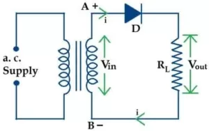
During the +ve half cycle of input end ‘A’ becomes +ve with respect to end ‘B’. This makes the diode forward bias and hence it conduct current. During the −ve half cycle end ‘A’ becomes −ve with respect to end ‘B’.
And this makes the diode revers bias and no current conducts. Therefore the current flow the diode during +ve half cycle only.
And through the load ‘RL‘ in the same direction. Hence the d. c. output is obtained across the load.

For What is semiconductor and its types click here.
Disadvantage
- The output is low, efficiency also less.
- The output is pulsating d. c. so we require filter circuit to get pure d. c.
Full wave rectifier –
In full wave rectification current flow through the load in the same direction for both half cycle of input a. c. voltage.
Therefore a full wave rectifier utilize both half cycle of input a. c. voltage to produce d. c. output. There are two types of full wave rectifier.
- Centre tap full wave rectifier
- Full wave bridge rectifier
Explain center tapped full wave rectifier

The circuit consist of two diodes D1 and D2 , and a center tapped secondary winding AB.
Diode D1 utilize the a. c. voltage appearing across the upper half of secondary winding and diode D2 us the lower half of secondary winding.
During the +ve half cycle the end ‘A’ becomes +ve with respect to ‘B’ and this makes diode D1 forward biased and diode D2 reverse biased. Therefore diode D1 conducts while diode D2 does not.
The current flow through the diode D1 low resistance ‘RL‘ and the upper half of winding is shown by the dotted arrow. During the −ve half cycle end ‘A’ becomes −ve with respect to ‘B’.
This makes diode D2 forward biased and D1 reverse biased. Therefore diode D2 conducts while D1 does not. The current flow through the diode D2 , low resistance ‘RL‘ .
And the lower half of the secondary winding is shown by solid arrow. The current flow through the low resistance ‘RL‘ in the same direction for both the half cycle of input a. c. voltage.
Therefore the d. c. output is obtained across the load for both the half cycle.
Advantages
- The d. c. output voltage are twice than the half wave rectifier.
- The efficiency is double than the half wave rectifier.
- The ripple factor is much less than the half wave rectifier.
Disadvantages
- It is difficult to locate the center tapped point on the secondary winding.
- The diodes must have high peak inverse voltage ( 2Vm ).
- The d. c. output is small as each diode utilize only one half of the transformer secondary voltage.
Explain full wave bridge rectifier

The circuit consist of 4 diodes D1 , D2 ,D3 , D4 and a load resistance. The diode are connect to a bridge and between two ends of the bridge, the load ( RL ) is connect. And the power supply is given to the diagonally opposite ends of the bridge.
During the +ve half cycle

During the +ve half cycle the end ‘A’ becomes the +ve with respect to ‘B’. And this makes the diodes D1 and D3 are forward bias, while diode D2 and D4 reverse bias.
Therefore only diodes D1 and D3 conduct and the current flows from the point ‘A’ to ‘B’ .Through the load resistance ( RL ) as shown in the dotted arrow. Hence the d. c. output is obtained across the load RL .
Read also this what is single stage transistor amplifier?
During the −ve half cycle

During −ve half cycle end ‘A’ becomes −ve with respect to ‘B’ and this makes diode D2 and D4 are forward bias while diode D1 and D3 are reverse bias.
Therefore only diodes D2 and D4 conduct. And the current flow through the load resistance ( RL ) as shown by solid arrow.
Hence d. c. output is obtain across the load RL .During the both the half cycle the current flow through the load in the same direction.
Advantages and disadvantages of full wave bridge rectifier
Advantages
- The need of center tap transformer is eliminate.
- The output is twice than the center tapped rectifier.
- The PIV (Peak Inverse Voltage) is one half of the center tap rectifier.
Disadvantages
- It requires 4 diodes.
- The current flow through the [ A → D1 → RL → D3 → B → A ].
Also read What is transistor in electronics
In this post we read what is rectifier and what are its type? Ans also read different types of rectifiers and their working , advantage , disadvantage. If you have any doubt then comment me, Thank you.