
In this article we are discus about the functional block diagram and pin description of 8253 or 8254 (PIT) Programmable Interval Timer.
The 8253 is a programmable universal timer design for use in microcomputer system. Hence it uses N-MOS technology with +5 volt supply and it has 24 pin. Below you can see the block diagram of 8253 and Pin diagram.
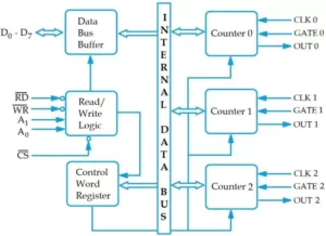
Block diagram of 8253
Read also this 8085 pin diagram
Pin diagram of 8253
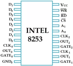
8253 pin description
RD – ( Read )
When this pin is low the CPU reads data.
WR – (Write )
When this pin is low CPU output data in the form of mode information or loading of counters.
A0 – A1
So These pins are connected to the address bus. So these pins are use for the selection of counters and control word register.
| A1 | A0 | Operation |
| 0 | 0 | Counter 0 operation |
| 0 | 1 | Counter 1 operation |
| 1 | 0 | Counter 2 operation |
| 1 | 1 | Control word operation |
CS – ( Chip Select )
So this pin is use in connection with A1 , A0 , WR, RD to determine different mode of operation.
| RD | WR | A1 | A0 | CS | Operation |
| 0 | 1 | 0 | 0 | 0 | Read counter 0 |
| 0 | 1 | 0 | 1 | 0 | Read counter 1 |
| 0 | 1 | 1 | 0 | 0 | Read counter 2 |
| 0 | 1 | 1 | 1 | 0 | No operation |
| 1 | 0 | 0 | 0 | 0 | Write into counter 0 |
| 1 | 0 | 0 | 1 | 0 | Write into counter 1 |
| 1 | 0 | 1 | 0 | 0 | Write into counter 2 |
| 1 | 0 | 1 | 1 | 0 | Write control word |
D0 – D7 – Bidirectional data bus
Data bus buffer
This buffer is within 8253. So it is a 3 – state bidirectional 8 bit buffer. Hence It is use to interface 8253 to the system data bus through D0 – D7 lines.
CLK
So CLK0 , CLK1 and CLK2 are clock for counter 0, counter 1 and counter 2 respectively.
GATE
So Gate0 , Gate1 and Gate2 are gate terminals for triggering purpose for counter 0, counter 1 and counter 2 respectively.
OUT
So OUT0 , OUT1 and OUT2 are output terminal of counter 0, counter 1 and counter 2 respectively.
Control word register
When the pins A0 , A1 are 11 the control word register is selected. So the control word format is shown below.

So The D7 and D6 bits of the control word register are use to select one of the three counters.
SC – ( Select counter )
So here to select the counter SC0 and SC1 are set as follows :
SC1 SC0
0 0 — Select counter 0
0 1 — Select counter 1
1 0 — Select counter 2
1 1 — Illegal
D5 – D4
So the D5 and D4 are use for loading or reading operation
RL – ( Read / Load )
To load / read counts RL0 and RL1 are set as follows :
RL1 RL0
0 0 — Counter latching operation
0 1 — Read / load least significant byte only
1 0 — Read / load most significant byte only
1 1 — Read / load least significant byte first then most significant byte
D3 – D2 and D1
So the D3– D2 and D1 are for the selection of operating modes of the selected counter.
Mode
So Mode selecting bits M0, M1 and M2 are set as follows :
| M2 | M1 | M0 | Operation |
| 0 | 0 | 0 | Mode 0 |
| 0 | 0 | 1 | Mode 1 |
| x | 1 | 0 | Mode 2 |
| x | 1 | 1 | Mode 3 |
| 1 | 0 | 0 | Mode 4 |
| 1 | 0 | 1 | Mode 5 |
D0
So D0 bit is use for the selection of binary or BCD counting. When D0 is set to 0 the selected counter operates as a binary counter and when it is set to 1 the counter operates as BCD counter.
BCD
- 0 binary counter 16 – bits.
- 1 binary coded decimal counter 4 decades.
Read also this Flags in 8085 microprocessor
Modes of operation of 8253
So the operational modes of INTEL 8253 are Mode-1, Mode-2, Mode-3, Mode-4 and Mode-5.
Mode – 0 ( Interrupt on terminal count )
Interrupt terminal count it is use for the generation of a counter time delay under software control. So one of the counter of 8253 is initialized and loaded with suitable count for the desired time delay,
When counting is over the counter interrupted the CPU. Hence on interrupt on the microprocessor perform the required task which is to be perform after desire time delay.
In Mode – 0 operation the output of the counter becomes initially low after the mode is set. So After mode set operation the counter is loaded with desired count N. Hence for mode – 0 operation GATE is always kept high and counting start.
If GATE is high while counting is going on the counter output (OUT) remains low. When the terminal count is reaches that is count reaches zero, the output becomes high and remains high until the count is reloaded.

Mode – 1 ( Programmable one shot )
So here the counter act as a retriggerable and programmable one shot. So the low to high transition of the signal applied to GATE as a trigger signal. In this mode of operation out signal become initially high after mode set operation.
So the counter is loaded by a count value of N. Then the counter decrements the counts and the output goes low for N clock cycle positive output goes low at the first negative edge of the GATE input.
The output remains low while the counting is going on. It goes high on terminals count ( That is counter counting = zero ) the width of the output pulse can be varying the output pulse.

Mode – 2 ( Rate Generator )
So here the counter act as a simple divide by N-Counter. The output of the counter becomes initially high. So After mode set operation the counter is loaded by a count of value N.
For mode – 2 operation the output remains high for (N-1) clock pulse and then goes low for 1 clock pulse. and After this the output becomes high again and the count N is automatically reloaded in to the counter.

Mode – 3 ( Square Wave Generator )
So here the counter act as a square wave generator. and after mode set operation the counter is loaded by a count of value N. So for mode – 3 operation GATE is kept high.
For even values of N the output remains high for N/2 clock pulse and then goes low for the next N/2 clock pulses.
So a continuous square wave is obtain for odd values of N. and The output remains high for N+1/2 clock pulse and low for N-1/2 clock pulses.

Mode – 4 ( Software Trigger Strobe )
In this mode – 4 operation the output of the counter becomes initially high after the mode is set. So GATE is kept high the counter begins counting immediately after the count is loaded into the count register.
When the counter reaches terminal count the output goes low for 1 clock period and then it returns to high.
This mode of operation is refers to as a software trigger strobe because the generation of strobe signal is trigger by loading the count into the count resister.

Mode – 5 ( Hardware trigger strobe )
So here the GATE input act as a trigger. After the mode is set output becomes initially high. and a count value of N is loaded into the counter. Hence the counting begins at the first negative edge of the clock after the rising edge of the GATE input.

What are features of 8253 ?
- 24 pin DIP (Dual inline package ).
- High speed and low power consumption is achieve using C – MOS technology.
- 3-independent 16-bit down counters.
- 6-counter modes available for each of the 3-counter.
From the above discussion, we came to know about the Intel 8253 (PIT) as well as what are its 5 types of modes. So I hope that I have given you complete information about Block diagram and pin configuration of 8253, Thank you.