
Here, we are going to talk about energy band diagram of conductor, insulator and semiconductor. We will also think a little bit about the energy band.
Solids may be insulators or conductors depending on the number of free electrons presents. All the solids can be classify into 3 types that is
- Conductor
- Insulator
- Semiconductor
Read also this what is semiconductor and its types
CONDUCTOR
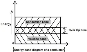
Conductors are the materials which can conduct electricity very easily. Hence, there are large number of free electrons present in a conductor. So, the valence band and conduction band in case of a conductor overlap each other. As the valence band and conduction band overlap each other. So the small potential difference can be apply to conduct electricity.
INSULATOR

Insulator are those materials which do not conduct electricity because they are negligible or free electrons. Hence, the energy difference between the valence band and conduction band. So, it is very high. ( ≃ 15 electron volt ) due to this the valency electrons require very high energy to become free from the pulling force of nucleus but this amount of high energy burns up the material rather then generating free electrons.
SEMICONDUCTOR

Semiconductor are the materials which do not conduct electricity at room temperature but if some impurity is add or temperature is raised then the semiconductor can conduct electricity easily. In this case the energy gap between valence band and conduction band So in a semiconductor is very less (Electron volt equal to one electron volt)
Definition energy level
It is defined as the energy possessed by the electrons of an atom.
Energy band definition
It is define as the range of energy possessed by all the electrons of all the atoms present in a material is know as energy band.
So there are two types of energy band (1) Valance band (2) Conduction band.

Valence band and conduction band definition
It is the range of energy acquired by the valence electrons of the atoms in a material, is know as valence band. It is the range of energy possessed by the free electrons in a material, is know as conduction band.
Now we know about forbidden energy gap.
For what is transistor in electronics? click here.
Forbidden energy gap
definition of forbidden energy gap : It is define as the energy difference between valence band and conduction band.

(i) Valence band :
In valence band, only valence electrons are present which are attach to the nucleus. So, these electrons are not responsible form current conduction.
(ii) Conduction band :
In conduction band , only free electrons or conduction electrons are present. So, these are responsible for conduction of current.
So friends, what did you learn in this article? Function of conductor, insulator and semiconductor. Here in the main role are free electrons. Free electrons are moving from the valence band to the conduction band.
The gap between the valence band and conduction band in a conductor is very small therefore current pass easily in it and many free electrons found in it. Just like that current does not pass easily in an insulator because the gap between the valence band and conduction band is very large. Semiconductor are similar to insulator, the only difference is that the gap between the valence band and conduction band is small.
I hope you like this article. share to your friends. Thank you.