
When a transistor to be connect in a circuit will require 4 terminals, 2 for the input and two for the output. We will share one terminal for both the input and output terminals and we will overcome this problem. So a transistor can be connect in three type configuration.
- Common base ( CB ) configuration
- Common emitter ( CE ) configuration
- Common collector ( CC ) configuration
Click for what is the filter circuit.
Click for types of electron emission.
Common base configuration of transistor
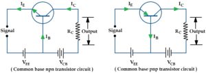
In this circuit arrangement input is apply between emitter and base. And output is taken from collector and base. Here the base and transistor is common both input and output circuit and hence the name is common base connection.
Current amplification factor ( α )
Here the output current is IC and input current is IE . It is the ratio between the change in collector current to the change in emitter current at constant VCB collector base voltage is know as current amplification factor α.
So current amplification factor α = ΔIC / ΔIE at constant VCB .The value of α ranges from 0.9 to 0.99.
Common base input characteristics
It is the curve between emitter current and emitter base voltage at a constant collector base voltage. IE is taken along y – axis and VBE taken along x – axis.

The emitter current IE increases rapidly with very small increasing emitter base voltage that means input resistance is very small. The emitter current is almost independent of collector base voltage VCB . So Input resistance ri = ΔVBE / ΔIE , at constant VCB .
Common base output characteristics
It is the curve between collector current IC and collector base voltage VCB at constant emitter current IE .Collector current is taken along y – axis and collector base voltage along x – axis.

The collector current varies with only at very low voltages and the transistor is never operate in this region. When the value of VCB is resist above 1 to 2 volt the collector current becomes constant. That means now IC is independent of VCB and depends upon IE only.
A very large change in collector base voltage produces only a small change in collector current. This means the output resistance very high.
So output resistance ro = ΔVCB / ΔIC , at constant IE .
Need information about What is single stage transistor amplifier
Common emitter configuration of transistor

In this circuit arrangement input is apply between base and emitter. And output is taken from the collector and emitter. Here the emitter is common to both in input and output. The common emitter connection has two characteristic.
- Input characteristic
- Output characteristic
Common emitter input characteristics

It is the curve between base current and base emitter voltage a constant collector emitter voltage.
Keeping VCE is constant the base current value note for various values of VBE .then plotting the readings taking IB along y – axis and VBE along x – axis. This characteristic same as the forward bias diode curve. As compare to common base IB increases less rapidly with VBE .
Therefore input resistance of a common emitter circuit is higher than common base circuit.
Input resistance ri = ΔVBE / ΔIB , at constant VCE . The value of input resistance is the order of a ( few 100 Ω )
Common emitter output characteristics

It is the curve between collector current and collector emitter voltage at constant base current IB . Keeping the base current IB constant and then collector current is note for various value of VCE .Then plotting the readings taking IC along y – axis and VCE along x – axis .
The collector current IC varies with VCE for VCE between 0 and 1Volt only after this IC becomes almost constant and independent of VCE .This value of VCE up to which collector current IC changes with VCE is called the knee voltage ( Vknee ).The transistor are always operated in the region above knee voltage.
However a small increase in IC with increasing VCE is cause by the collector depletion layer getting and capture in a few of more majority charge carrier before hole.
For any value of VCE above knee voltage collector current IC ≅ β × IB .Where β is the current amplification factor for common emitter connection.
Output resistance ro = ΔVCE / ΔIC at constant IB .So the output resistance is the order of 50 kΩ.
current amplification factor ( β )
In Common emitter connection input current is IB and output current IC . Current amplification factor β is defined as the ratio between change in collector current to the change in base current.
So the current amplification factor is β = ΔIC / ΔIB
What is CC configuration (Common Collector Configuration)

In this configuration input signal is apply between base and collector. And output is taken across the emitter and collector. Here the collector is common to both input and output circuit. So the name common collector configuration. The common collector configuration also has two characteristic.
- Input characteristic
- Output characteristic
Common collector input characteristics

It is the curve between base current and base collector voltage a constant emitter collector voltage . Here in this curve the input variable is IB , VCB and the output variable VCE is present.
IB = Input Current , VCB = Input Voltage , VCE = Output Voltage
Keeping VCE is constant at 2V and the base current value is note for various value of VCB Then plotting the readings taking IB along y – axis and VCB along x – axis. We again keeping VCE is constant at 4V and note down the base current value for different values of VCB, then plot the readings.
Common collector output characteristics
It is the curve between emitter current IE and emitter collector voltage VCE at constant base current IB . So in this curve we get 3 regions you can see in the graph.

So first we will keep the base current IB as constant and note the emitter current IE for various value of VCE . Now we will increase the base current from 0.
When the base current is 0 then the transistor also 0 no current will flow, so we call it cut off region. Now the base current is 0, so we will gradually increase it from 0 to 5 μA, after that 10 μA, 15 μA like this, so from this we will call active region. And now the value of IB = 20 μA it means a lot of current is flowing, so obviously the transistor will also have a lot of current flowing through it, due to which we call saturation region.
See also this What is multistage transistor amplifier
Current amplification factor gamma ( γ )
The ratio of change in emitter current (Δ IE ) to the change in base current (Δ IB ) in know as the current amplification factor γ. So the current amplification factor γ = Δ IE / Δ IB .
Total collector current IC = α IE + I leakage, ‘I’ represent I leakage = ICBO ( ICBO = Collector base current with emitter open ) So now we can write IC = α IE + ICBO Expression for collector current
IC = α IE + ICBO
We know IE = IB + IC
IC = α (IB + IC ) + ICBO = α IB + α IC + ICBO
IC – α IC = α IB + ICBO
So now we take common IC
IC ( 1 – α ) = α IB + ICBO
IC = α IB / (1 – α ) + ICBO / (1 – α )
So it is about transistor configuration it is basically 3 type of configuration and 2 characteristics input output, I hope you will understand very well which i explain, If you have any doubt from this then comment me and share to your friends, Thank you.