
A transistor power amplifiers handles large signals. Many of those inputs are driven so hard by the large signal that the collector current either cut-off or is in the saturation region during a large portion of the input cycle.
Therefore, such amplifiers are generally classified according to their mode of operation, that is the part of the input cycle during which the collector current is expected to flow. On this basis, power amplifiers are classified as follows :
- Class A power amplifier
- Class B power amplifier
- Class C power amplifier
See also this : What is transistor audio power amplifier?
What is Class A power amplifier
If collector current flows at all times during a complete cycle of the signal, the power amplifier will be call a Class A power amplifier.
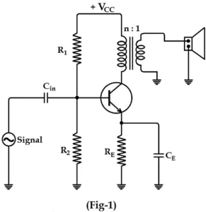

For this to happen, the power amplifier must be biased in such a way that no part of the signal is cut off. In figure (1) you can see the circuit of class A power amplifier.
Note that the collector has a transformer as the load which is most common for all classes of power amplifiers. The use of transformers allows impedance matching, resulting in maximum power transfer to the load, (for example loudspeaker).
In figure (2) we can see class A operation with reference to A. C. load line. The operating point Q is chosen such that collector current flows at all times throughout the entire cycle of the applied signal.
Since the output wave shape is exactly the same as the input wave shape, therefore, there is least distortion in such amplifiers. However, they have the disadvantages of low power output and low power efficiency (about 35%).
See also this : What is Multistage Transistor Amplifier?
What is a Class B power amplifier?
If collector current flows only during the positive half cycle of the input signal, it will be call a Class B power amplifier.

In class B operation, the transistor bias is adjusted such that the zero signal collector current is zero that is, no biasing circuit is needed at all.
During the positive half-cycle of the signal, the input circuit is forward bias and hence collector current flows. However, during the negative half-cycle of the signal, the input circuit is reverse biased and no collector current flows. In the picture above we can see Class B operation with reference to an A. C. load line.
Obviously, the operating point Q will be located at the collector cut-off voltage. It is easy to see that the output from a Class B amplifier is amplified by half-wave rectification.
The negative half-cycle of the signal is cut-off in a Class B amplifier, and therefore a severe distortion occurs. However, higher power output and power efficiency (50-60%) are provided by Class B amplifiers. Such amplifiers are mostly used in push-pull arrangement for power amplification.
In this type of arrangement, 2 transistors are use in class B operation. One transistor amplifier amplifies the positive half-cycle of the signal while other transistor amplifiers amplifies the negative half-cycle.
See also this : What is Single Stage Transistor Amplifier?
What is Class C power amplifier?
If the collector current flows for less than half-cycle of the input signal, it will be call a class C power amplifier.
In class C amplifier, the base is given some negative bias so that the collector current does not flow when the positive half cycle of the signal begins. Such amplifiers are never use for power amplification.
However, they are use as tuned amplifiers. That is to amplify a narrow band of frequencies near the resonant frequency.
What is the maximum power efficiency of series fed Class A power amplifier?


What is the maximum power efficiency of a transformer coupled Class A power amplifier?
In a Class A power amplifier, the load may be either directly coupled to the collector or it may be transformer-coupled. The latter method is often prefer for two main reasons.
First, transformer coupling allows impedance matching and second it keeps D. C. power losses small due to the small resistance of the transformer primary winding.
In figure – 1 you can see a transformer-coupled Class A power amplifier. To determine maximum power efficiency, refer to the output characteristic shown in figure-2. Under zero signal conditions, the effective resistance in the collector circuit is that of the primary winding of the transformer.
![]()

The value of primary resistance is very small and it is take as zero. Therefore, the D. C. load line is a vertical line rising above VCC as you can see in figure-2. When a signal is applied, the collector current will vary about the operating point Q.
To obtain maximum A. C. power output, the peak value of the collector current due to the signal alone must equal the zero signal collector current IC. With reference to an A. C. load line, the operating point Q must be located at the center of the A. C. load line.
Expression for maximum power efficiency of a transformer coupled Class A power amplifier
During the peak of the positive half-cycle of the signal, the total collector current will be 2 IC and vce = 0. And during the negative peak of the signal, the collector current will be zero and vce = 2VCC.
Therefore, the peak to peak collector-emitter voltage is vce(P −P) = 2VCC
And peak to peak collector current is, ic(p − p) = 2 IC
![]()
Where R’L is the reflected value of load RL and appears in the primary of the transformer. If n ( = NP /NS) is the turns ratio of the transformer, then R’L = n2 RL.
D. C. power input is, Pdc = VCC IC
= I2C R’L
Maximum A. C. output power, Po(max) =
![]()
![]()
![]()
Maximum power (η) =
![]()
See also this : Four bit ripple counter – What is 4-bit ripple counter?
Maximum efficiency of class B power amplifier
We have already seen that a push-pull circuit uses two transistors that operate in class B operation. For Class B operation the Q-point is located at the cut-off on both the D. C. and A. C. load lines.
For maximum signal operation, the two transistors in a Class B amplifier are alternately operate from cut-off to saturation. You can see it in figure-1.


It is clear that A. C. output voltage has a peak value of VCE and A. C. output current has a peak value of IC(sat). The same information is also passed through the A. C. load line to the circuit (see figure-2).
Therefore, Peak A. C. output voltage is = VCE
Peak A. C. output current = IC (sat) = VCE / RL = VCC / 2 RL
Maximum average A. C. output power Po (max) is
Po (max) = Product of r.m.s. value of A. C. output voltage and A. C. output current


Therefore, Po (max) = 0.25 VCC IC (sat)
The input D. C. power from the supply VCC is
Pdc = VCC Idc
Where Idc is the average current taken from the supply VCC. Since the transistor is on for alternating half-cycles, this efficiency acts as a half-wave rectifier.
Idc = IC(sat) / π
Pdc = VCC IC(sat) / π
Maximum power (η) =

= 0.25 π × 100 = 78.5%
See also this : Explain push pull amplifier